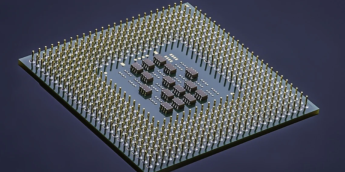



The relentless pursuit of smaller, faster, and more energy-efficient microchips has driven decades of innovation in semiconductor technology, but we’re rapidly approaching fundamental physical limits. Shrinking integrated circuit (IC) dimensions presents increasingly complex challenges – a problem that’s pushing the boundaries of what’s possible with traditional manufacturing techniques. As feature sizes continue to decrease, the masks used to pattern these intricate designs become exponentially more difficult and expensive to produce. Current mask optimization processes are largely rule-based and iterative, often relying on human expertise and struggling to account for the vast number of variables involved in modern lithography. This leads to suboptimal patterns, increased manufacturing defects, and ultimately, higher costs. Enter MaskOpt: a groundbreaking solution poised to redefine AI chip manufacturing. Developed by, this innovative platform leverages advanced artificial intelligence algorithms to drastically improve mask design optimization, unlocking new levels of performance and efficiency in the semiconductor fabrication process. It promises a significant leap forward in overcoming the limitations we currently face.
The Problem with Traditional Mask Optimization
The relentless push for smaller, more powerful integrated circuits (ICs) has led to a critical bottleneck in chip manufacturing: mask optimization. Traditional optical lithography, the technique used to transfer circuit designs onto silicon wafers, faces increasing challenges as feature sizes approach and even fall below the wavelength of light used. This shrinking window introduces significant diffraction effects – essentially bending and scattering of light – which distort the intended patterns on the wafer. These distortions aren’t uniform either; process variability introduced by manufacturing imperfections further complicates matters, leading to inconsistent chip performance.
To combat these issues, engineers rely heavily on Optical Proximity Correction (OPC) and Inverse Lithography Technique (ILT). OPC involves pre-distorting the mask design to compensate for diffraction effects during lithography. ILT takes a reverse approach, attempting to determine the original mask pattern needed to achieve the desired wafer pattern after accounting for optical distortions. While vital for producing functional chips, these techniques are incredibly computationally demanding. Each iteration of OPC or ILT requires running complex simulations that model light propagation and material interactions, consuming vast amounts of processing power and time.
The computational cost associated with traditional OPC/ILT is a major impediment to scalability in chip manufacturing. As designs become more intricate and feature sizes shrink further, the number of simulations needed explodes, significantly slowing down the design cycle and increasing development expenses. Simply put, existing methods struggle to keep pace with the demands of modern IC fabrication, creating a need for innovative solutions that can accelerate and improve the mask optimization process.
While deep learning has begun to show promise in tackling this challenge, previous approaches have been hampered by limitations. Many rely on synthetic datasets which lack the nuances of real-world chip layouts, ignore the hierarchical structure of standard cells (pre-designed building blocks), and fail to consider the surrounding context crucial for accurate mask optimization. This restricted scope limits their effectiveness when applied to actual manufacturing scenarios, highlighting the need for a more comprehensive and practical AI-driven solution.
Optical Lithography’s Shrinking Window

The relentless pursuit of smaller and more powerful integrated circuits (ICs) has pushed optical lithography – the process used to transfer circuit designs onto silicon wafers – to its physical limits. As feature sizes shrink below the wavelength of light used for exposure, diffraction effects become increasingly prominent. Diffraction causes light waves to bend around edges, blurring the intended patterns on the wafer and leading to variations in critical dimensions. These dimensional inaccuracies can severely impact IC performance and yield.
To counteract these diffraction-related issues, engineers employ Optical Proximity Correction (OPC). OPC involves pre-distorting the mask – a master template used in lithography – to compensate for the distortions introduced by light diffraction during exposure. Inverse Lithography Technique (ILT) is another sophisticated correction method that attempts to directly solve for the optimal mask shape based on desired wafer patterns. However, both OPC and ILT are computationally intensive processes, requiring numerous simulations and iterations to achieve acceptable results.
The computational burden of OPC and ILT significantly restricts their scalability. Each simulation can take hours or even days to complete, especially when dealing with complex chip designs. This bottleneck limits the ability to efficiently optimize masks for increasingly intricate ICs, highlighting a critical need for faster and more effective mask optimization techniques.
Introducing MaskOpt: A New Benchmark Dataset
The pursuit of ever-smaller, more powerful microchips has hit a significant roadblock in optical lithography – the process used to transfer designs onto silicon wafers. As feature sizes shrink below the wavelength of light, diffraction effects become increasingly problematic, requiring complex and computationally intensive techniques like Optical Proximity Correction (OPC) and Inverse Lithography Technique (ILT). These methods are essential for ensuring accurate chip fabrication but dramatically slow down the design cycle. Recent efforts to leverage Artificial Intelligence (AI) in mask optimization have shown promise, however, their effectiveness has been hampered by limitations inherent in existing datasets.
Current AI-driven approaches often rely on synthetic layouts generated without mirroring real-world complexities. These simulated environments frequently lack crucial details like standard-cell hierarchy – the modular building blocks of modern chips – and fail to account for the surrounding context around the mask optimization targets. This disconnect means models trained on these datasets struggle to generalize to actual manufacturing scenarios, hindering their practical applicability. Simply put, they’re learning from a fundamentally flawed representation of reality, limiting their potential to truly revolutionize AI chip manufacturing.
Enter MaskOpt: a new benchmark dataset designed specifically to address these shortcomings. Unlike previous offerings, MaskOpt incorporates data derived from real-world standard cells and includes extensive contextual information surrounding the optimization regions. This allows for training AI models that are more attuned to the complexities of practical mask optimization tasks. The dataset’s structure emphasizes cell hierarchy and provides a richer representation of manufacturing constraints, paving the way for more robust and scalable deep learning solutions in this critical area.
By providing a significantly improved foundation for AI model development, MaskOpt aims to accelerate progress towards more efficient and accurate chip manufacturing processes. This new resource represents a crucial step forward in bridging the gap between research and real-world application, ultimately enabling faster innovation and pushing the boundaries of what’s possible in AI chip manufacturing.
Why Existing Datasets Fall Short

Previous attempts to leverage artificial intelligence (AI) in chip manufacturing, specifically for mask optimization, have been hampered by significant limitations in available training data. Many early efforts relied heavily on synthetic layouts generated using simplified models of the fabrication process. While useful for initial experimentation, these datasets lacked the complexity and variability found in real-world IC designs, preventing AI models from generalizing effectively to actual production scenarios.
A further constraint stemmed from a lack of awareness regarding the hierarchical structure inherent in modern integrated circuits. Standard cells—pre-designed building blocks used repeatedly within an IC—are organized into intricate hierarchies. Existing datasets often treated each cell as isolated, ignoring how changes made to one cell can impact neighboring cells and overall circuit performance. This absence of hierarchical understanding severely restricted the ability of AI models to optimize masks holistically.
Beyond individual cells, contextual information surrounding the target areas for mask optimization was frequently absent in prior datasets. Features like metal routing layers or adjacent transistors significantly influence lithographic behavior; neglecting this broader context led to suboptimal results and limited the practical applicability of AI-driven mask optimization solutions.
Key Features of the MaskOpt Dataset
The MaskOpt dataset represents a significant leap forward in enabling AI chip manufacturing through deep learning. Unlike previous attempts that relied on purely synthetic layouts or lacked crucial real-world complexity, MaskOpt is designed to bridge the gap between research and practical mask optimization workflows. Its sheer scale – encompassing over 104,000 metal tiles and 121,000 via tiles – provides a robust foundation for training sophisticated AI models capable of tackling the intricate challenges inherent in modern chip fabrication.
A key differentiator for MaskOpt is its structure, which meticulously incorporates standard-cell placement. Standard cells are fundamental building blocks of integrated circuits, and failing to account for their hierarchical organization severely limits the applicability of any resulting model. The dataset not only includes these standardized components but also preserves their spatial relationships within larger circuit designs. This allows AI models to learn how mask optimizations affect entire functional units rather than just isolated features.
Beyond individual cells, MaskOpt introduces a crucial element often missing from prior datasets: contextual awareness. Each tile is associated with surrounding ‘context windows,’ providing the model with information about its neighbors and the overall circuit layout. This context is vital because mask optimization decisions rarely impact only a single area; they require considering global effects to minimize distortions and ensure manufacturability. The inclusion of these context windows allows for more holistic and accurate AI-driven optimizations.
Ultimately, MaskOpt’s combination of scale, structured data incorporating standard cells, and the inclusion of context windows paves the way for deep learning models that can truly revolutionize AI chip manufacturing processes. By providing a dataset that more closely mirrors real-world scenarios, researchers can now develop and refine algorithms capable of significantly reducing computational costs and improving the quality of manufactured chips.
Scale and Structure: Tiles, Cells, and Context
The MaskOpt dataset is designed to address the limitations of existing datasets for AI chip manufacturing by offering a significantly larger scale and more realistic structure. It comprises over 104,000 metal tiles and 121,000 via tiles, representing a substantial increase in data volume compared to prior efforts. This expanded size allows for training more robust and generalizable deep learning models aimed at optimizing masks used in chip fabrication.
Crucially, MaskOpt incorporates standard-cell placement information which is vital for real-world mask optimization scenarios. Unlike many previous datasets that rely on purely synthetic layouts, MaskOpt reflects the hierarchical nature of integrated circuits by including data related to how standard cells are arranged and connected within a larger design. This facilitates training models capable of understanding and adapting to common chip architectures.
Furthermore, the dataset utilizes context windows around each mask optimization target. These windows provide surrounding layout information, allowing models to learn dependencies and relationships beyond the immediate area being optimized. By considering this broader context, MaskOpt enables the development of AI solutions that can more accurately account for complex interactions during the lithography process and ultimately improve chip manufacturing yields.
Impact & Future Directions
MaskOpt’s emergence represents a significant step forward in AI chip manufacturing by directly addressing the escalating computational burdens inherent in optical proximity correction (OPC) and inverse lithography technique (ILT). The reliance on iterative, simulation-heavy processes has historically bottlenecked scalability in chip fabrication. By leveraging deep learning to optimize masks – essentially the templates used to etch circuit patterns onto silicon wafers – MaskOpt promises a pathway towards faster design cycles and potentially improved chip performance. The initial benchmarking results underscore this potential, demonstrating that context size and cell awareness are critical factors influencing model effectiveness; models that ignore these aspects simply cannot achieve comparable accuracy or efficiency in real-world scenarios.
The implications of this technology extend beyond mere speed improvements. Traditional OPC/ILT methods often struggle to fully account for the complex interplay between different circuit elements, leading to subtle but impactful variations in chip behavior. MaskOpt’s cell-aware and context-sensitive approach allows it to better capture these nuances, potentially unlocking opportunities for more aggressive design rules and increased transistor density – key drivers of improved AI hardware performance. This is particularly crucial as we push towards ever smaller feature sizes where diffraction effects become increasingly dominant.
Looking ahead, several exciting research directions emerge from the MaskOpt framework. Further exploration into generative adversarial networks (GANs) could potentially create even more realistic and diverse training datasets, moving beyond reliance on purely synthetic data. Integrating reinforcement learning techniques might allow for adaptive mask optimization strategies that dynamically adjust to changing process conditions during manufacturing. Moreover, extending MaskOpt’s capabilities to handle 3D chip architectures and advanced packaging technologies presents a formidable but rewarding challenge, promising even greater advancements in AI chip manufacturing.
Finally, the success of MaskOpt highlights a broader trend: the increasing integration of AI not just *within* chips (as processing power) but also *in the fabrication process itself*. This feedback loop – using AI to design and manufacture increasingly sophisticated AI hardware – has the potential to accelerate innovation across the entire semiconductor ecosystem. Future research will likely focus on developing more robust and explainable AI models for mask optimization, ensuring both high performance and a deeper understanding of their decision-making processes within this critical manufacturing process.
Benchmarking and Trade-offs
Initial evaluations of MaskOpt revealed a nuanced landscape regarding deep learning model performance in mask optimization. While various architectures like U-Nets and Transformers demonstrated promise, significant trade-offs emerged. Smaller models with limited context sizes exhibited faster training times but struggled to accurately predict complex diffraction patterns, particularly when dealing with intricate layout geometries. Conversely, larger Transformer models, capable of processing broader contextual information, achieved higher accuracy but at the cost of substantially increased computational resources and longer training durations.
A key finding highlighted the critical importance of ‘cell awareness’ – the ability for a model to understand and leverage the standardized structure of integrated circuit cells. Models trained without this knowledge frequently produced suboptimal results, often requiring extensive post-processing corrections. Furthermore, neglecting surrounding context proved detrimental; accurately predicting mask features necessitates considering their interaction with neighboring elements, reinforcing the need for models capable of capturing long-range dependencies across the entire layout.
These early benchmarks underscore that achieving practical applicability in AI chip manufacturing requires a careful balance between model complexity, computational cost, and architectural design. Future research will focus on developing more efficient Transformer variants, exploring techniques to incorporate cell awareness directly into training data generation, and investigating methods for dynamically adjusting context size based on the specific optimization challenge.
The emergence of tools like MaskOpt signals a profound shift in how we approach complex engineering challenges, particularly within AI chip manufacturing. This isn’t just about incremental improvements; it represents a paradigm change fueled by the power of accessible machine learning techniques. The ability to optimize intricate processes previously reliant on human expertise and lengthy simulations holds immense promise for reducing costs, accelerating timelines, and ultimately democratizing access to cutting-edge technology. MaskOpt’s success underscores that AI isn’t just transforming what we *do*, but how we *do* it, fundamentally reshaping industries from the ground up. We believe this is only the beginning of a wave of intelligent tools designed to optimize every facet of modern fabrication. The implications for future generations of processors and the broader technological landscape are truly exciting and warrant continued attention. To further propel these advancements and unlock even greater potential, we invite you to delve into the dataset underpinning MaskOpt’s development – it’s freely available and ripe with opportunity. Join us in shaping the next generation of innovation by exploring the data, experimenting with your own models, and contributing to a collaborative future for AI chip manufacturing research; your insights could be instrumental in pushing these boundaries even further.
Your contributions, whether through novel algorithms or insightful analyses, will help refine our understanding and accelerate progress. We strongly encourage researchers, engineers, and enthusiasts alike to engage with the dataset and share their findings – let’s build upon this foundation together!
Source: Read the original article here.
Discover more tech insights on ByteTrending ByteTrending.
Discover more from ByteTrending
Subscribe to get the latest posts sent to your email.